Altium 18 Remove Rooms
Room Altium Nexus 2 0 User Manual Documentation

Layer Stack Manager Altium Designer 18 1 User Manual Documentation
Altium Error What Is This Reddish Box Electrical Engineering Stack Exchange
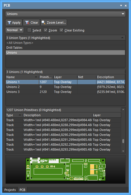
Pcb Unions Altium Designer 18 1 User Manual Documentation
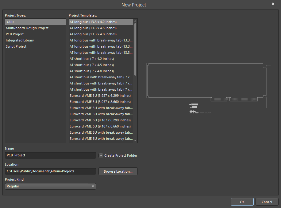
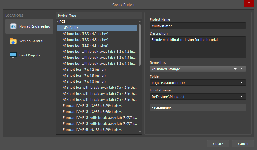
New Project Altium Designer 18 1 User Manual Documentation
Open Project Altium Designer 19 1 User Manual Documentation

A room is a primitive design object.
Altium 18 remove rooms.
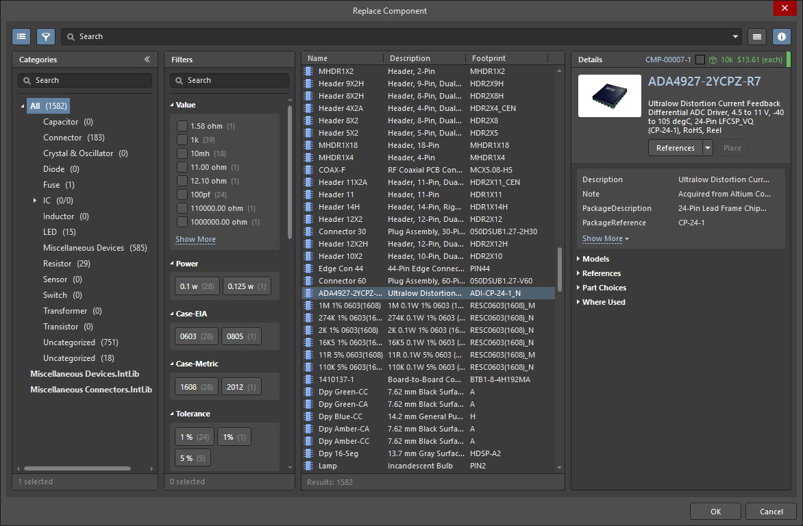
Replace Component Managed Altium Nexus 3 2 User Manual Documentation
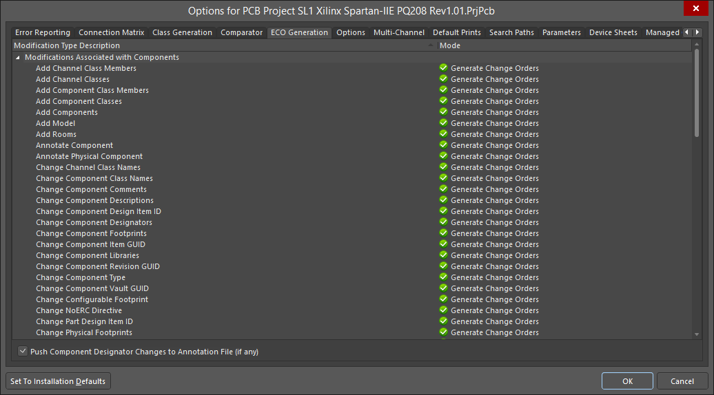
Project Options Eco Generation Altium Designer 18 1 User Manual Documentation

Bom Management With Activebom Altium Designer 20 2 User Manual Documentation
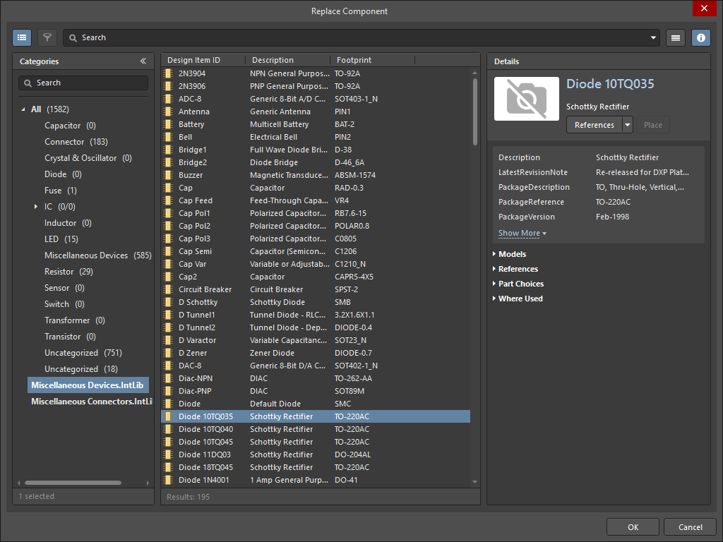
Replace Component File Based Altium Designer 20 2 User Manual Documentation
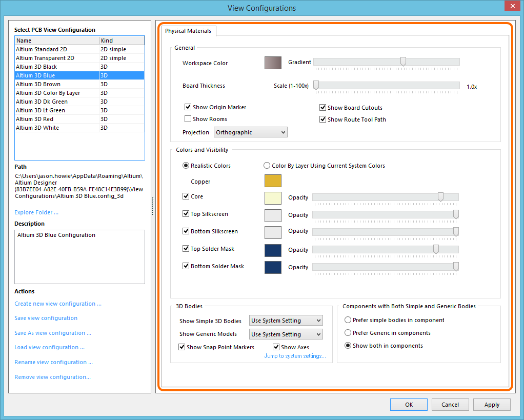
View Configurations Physical Materials Tab Altium Designer 18 1 User Manual Documentation
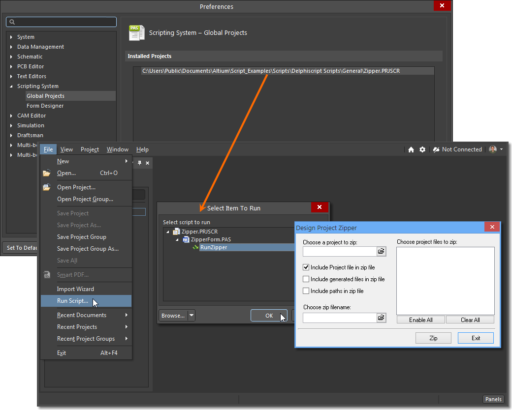
Running Scripts Altium Designer 20 2 User Manual Documentation

Query Helper Pcb Altium Designer 20 2 User Manual Documentation
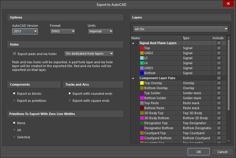
Export To Autocad Pcb Altium Designer 20 2 User Manual Documentation
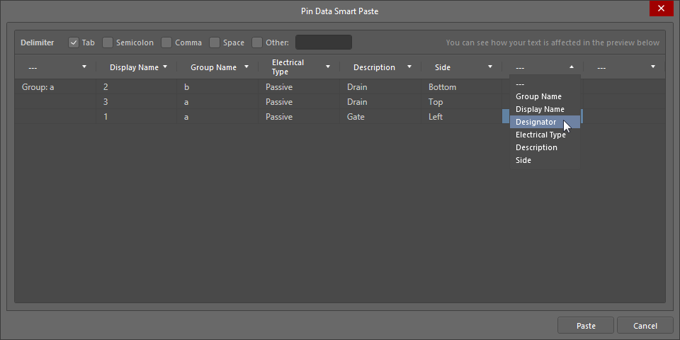
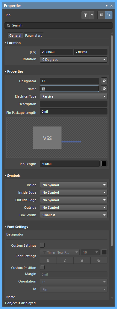
Pin Data Smart Paste Altium Designer 20 2 User Manual Documentation
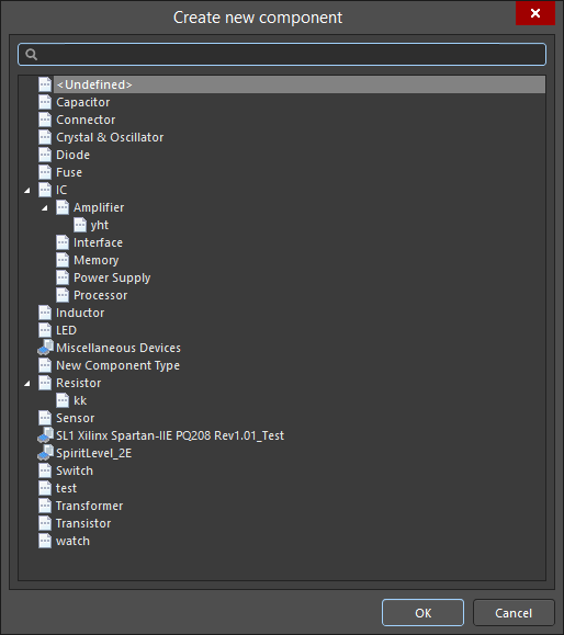
Create New Component Altium Designer 18 1 User Manual Documentation
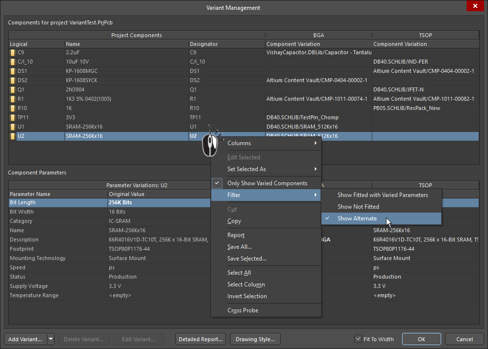
Design Variants Altium Nexus 1 1 User Manual Documentation

Pick And Place Setup Altium Designer 20 0 User Manual Documentation
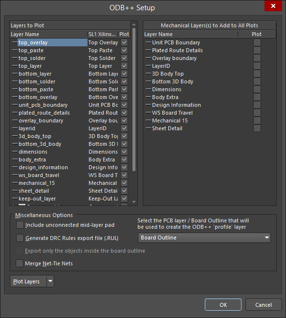
Odb Setup Altium Designer 20 0 User Manual Documentation
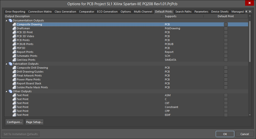
Project Options Default Prints Altium Designer 18 1 User Manual Documentation
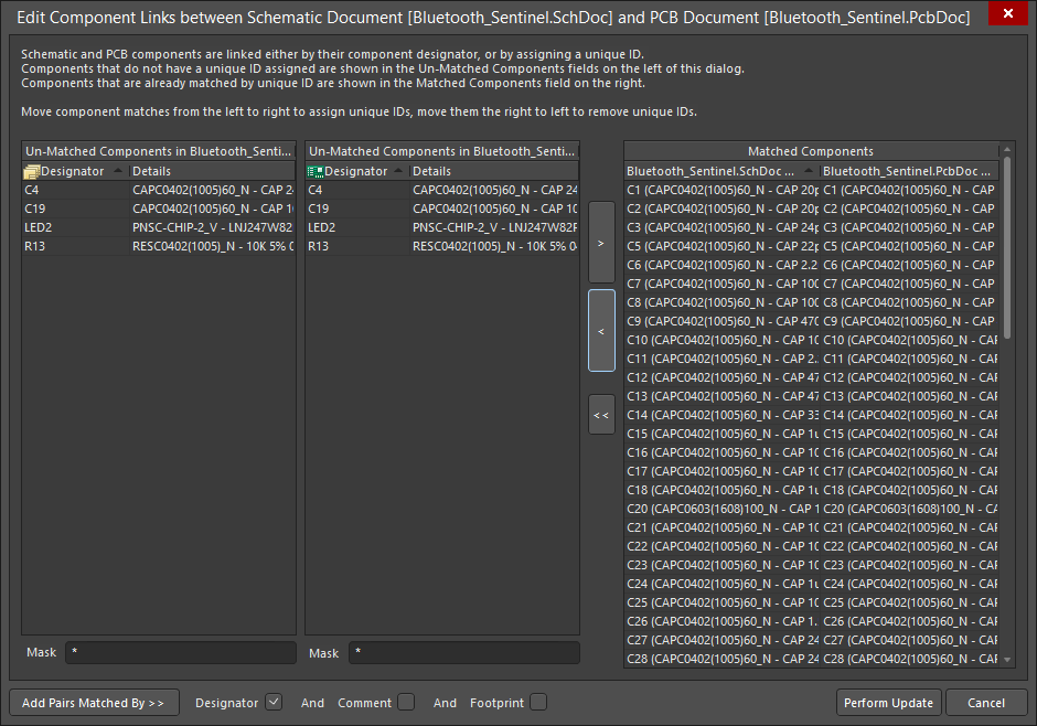
Edit Component Links Altium Nexus 3 2 User Manual Documentation
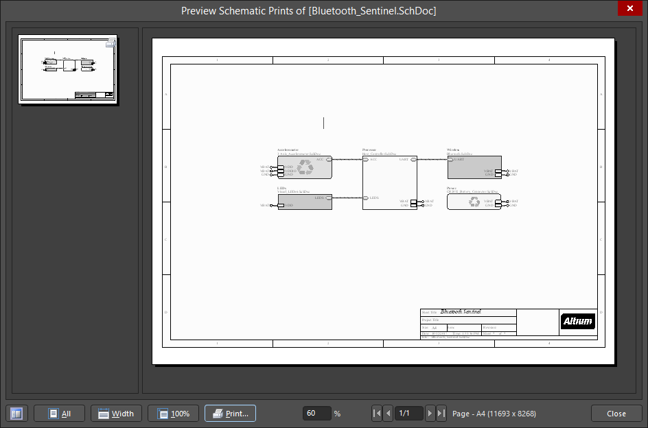
Print Preview Altium Designer 19 0 User Manual Documentation
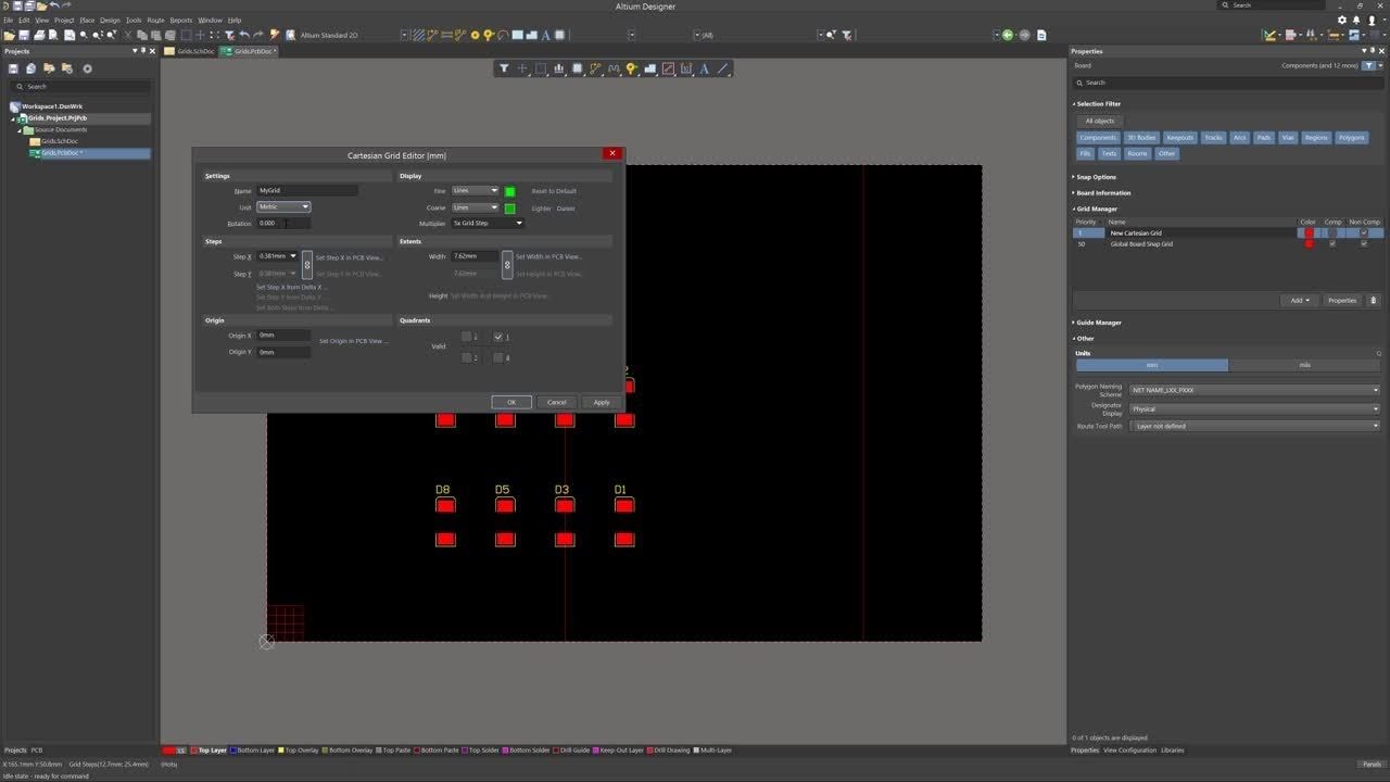
Pcb Grids Altium Designer 19 Essentials Module 18 Youtube
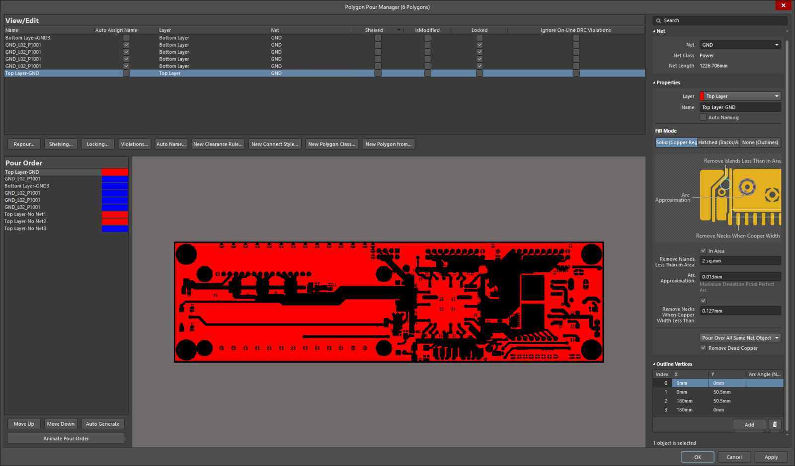
Polygon Pour Manager Altium Designer 19 1 User Manual Documentation
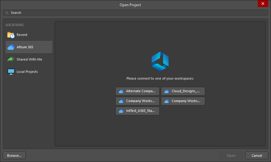
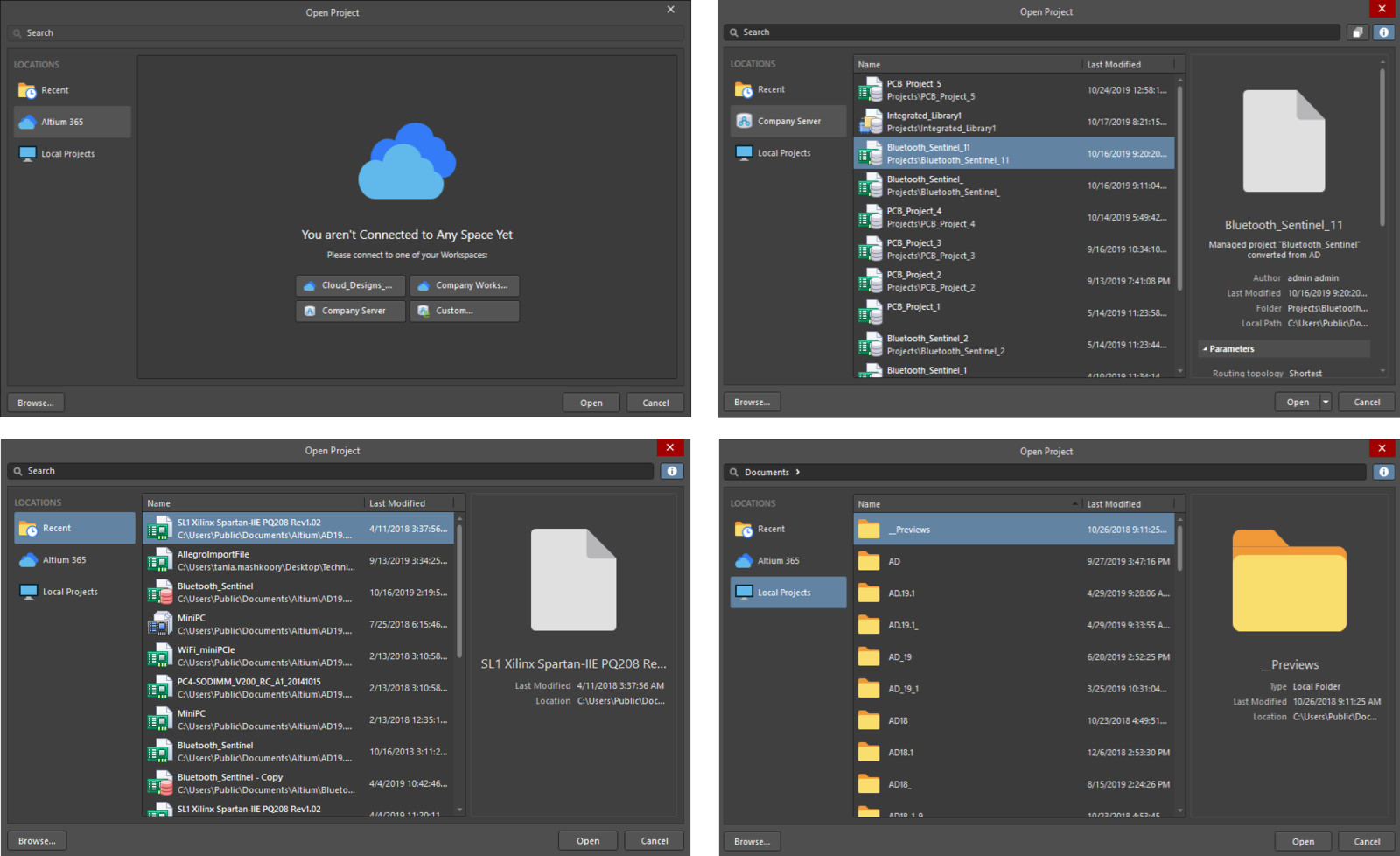
Open Project Altium Designer 20 2 User Manual Documentation

Report Preview Altium Designer 18 0 User Manual Documentation
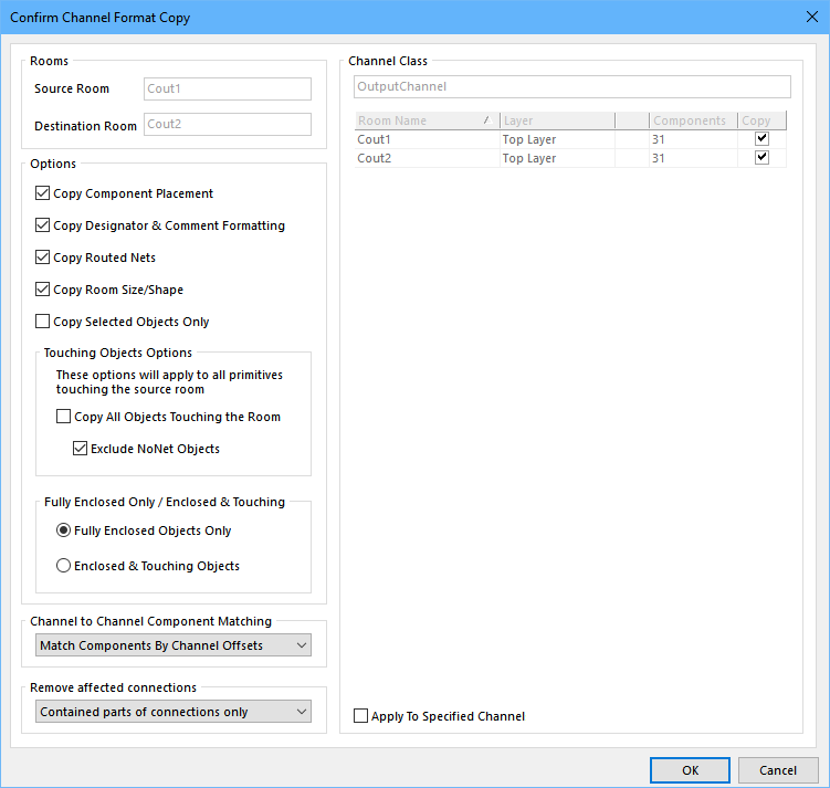
Confirm Channel Format Copy Altium Designer 18 0 Rukovodstvo Polzovatelya Dokumentaciya
Component Display Properties Altium Designer 20 2 User Manual Documentation
From Idea To Manufacture Driving A Pcb Design Through Altium Nexus Altium Nexus 1 1 User Manual Documentation
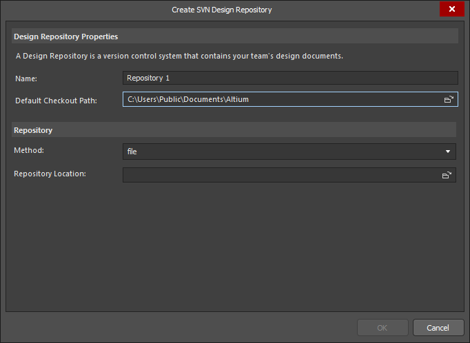
Create Svn Design Repository Altium Designer 20 2 User Manual Documentation

Altium Designer Lets You Easily Adjust Settings On Your Pcb Solder Mask
A Look At Creating Library Components Altium Designer 18 0 User Manual Documentation

Pin On Free Software
Board Shape Altium Designer 20 2 User Manual Documentation

Altium How To Copy Placement Without Using Rooms Or Channels Youtube

Advanced Layer Stack Manager In Altium Designer Youtube

Defining The Pcb Shape Altium Designer 19 Essentials Module 17 Youtube
From Idea To Manufacture Driving A Pcb Design Through Altium Nexus Altium Nexus 2 0 User Manual Documentation
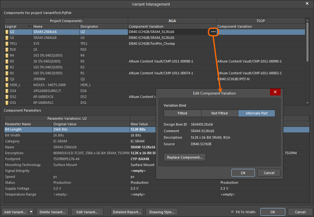
Design Variants Altium Nexus 3 2 User Manual Documentation

Altium Designer Tutorial 6 For Beginners Auto Route Unroute Youtube

Bill Of Materials Generation With Activebom Altium Designer 19 Essentials Module 27 Youtube

Pcb Placement Altium Designer 19 Essentials Module 20 Youtube

How To Edit Copper Polygons On Your Pcb Layout On Altium Designer 17 Pcb Design Software Youtube
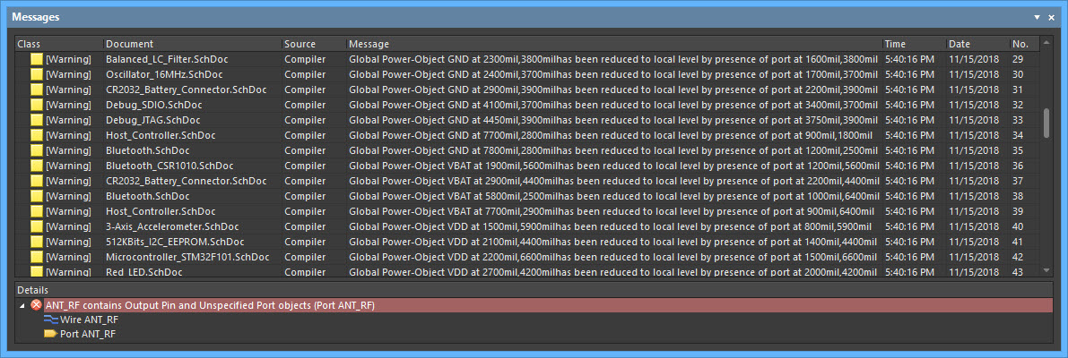
Messages Altium Designer 20 2 User Manual Documentation
Gnss Lte Asset Tracker Project Part 2 Altium Designer Project
Activeroute Altium Designer 20 2 User Manual Documentation
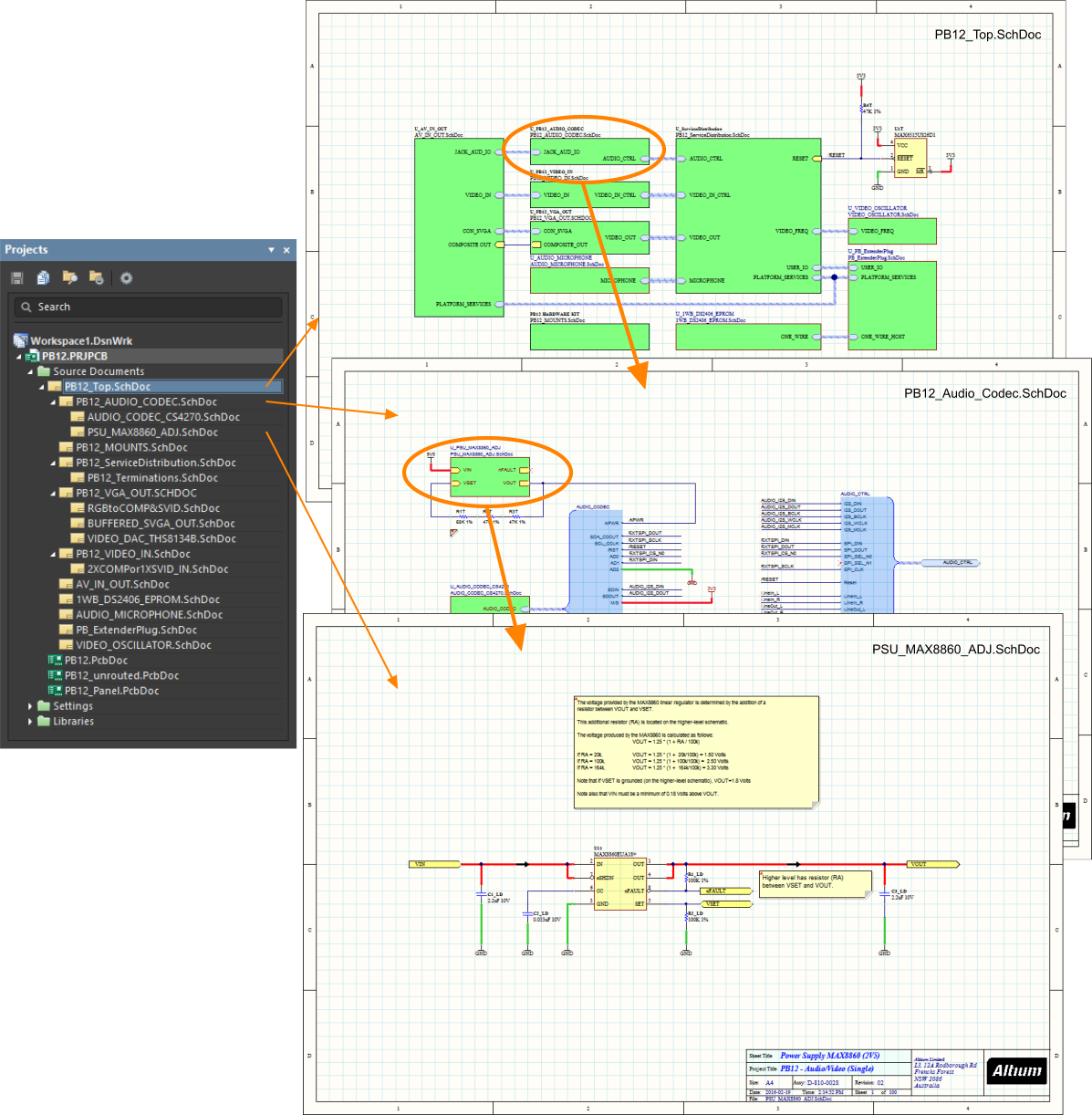
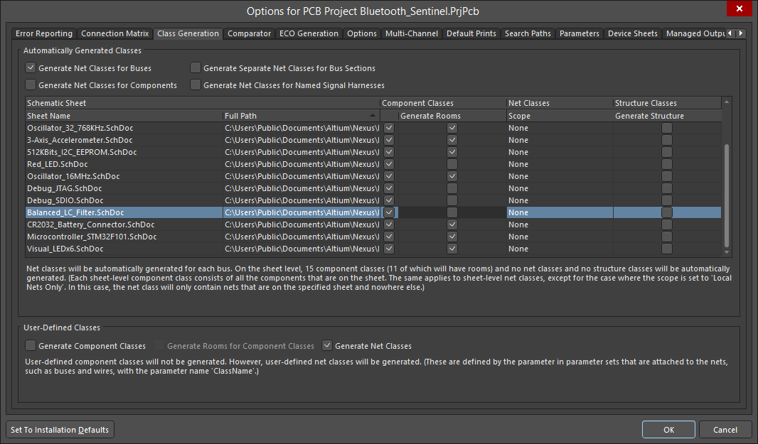
Multi Sheet And Multi Channel Design Altium Designer 18 1 User Manual Documentation
Design Synchronization Altium Designer 18 1 User Manual Documentation
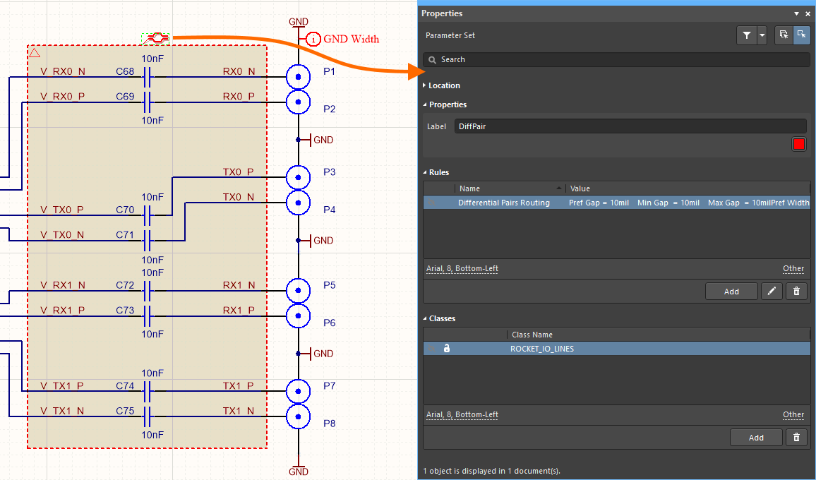
Differential Pair Routing Altium Designer 18 1 User Manual Documentation
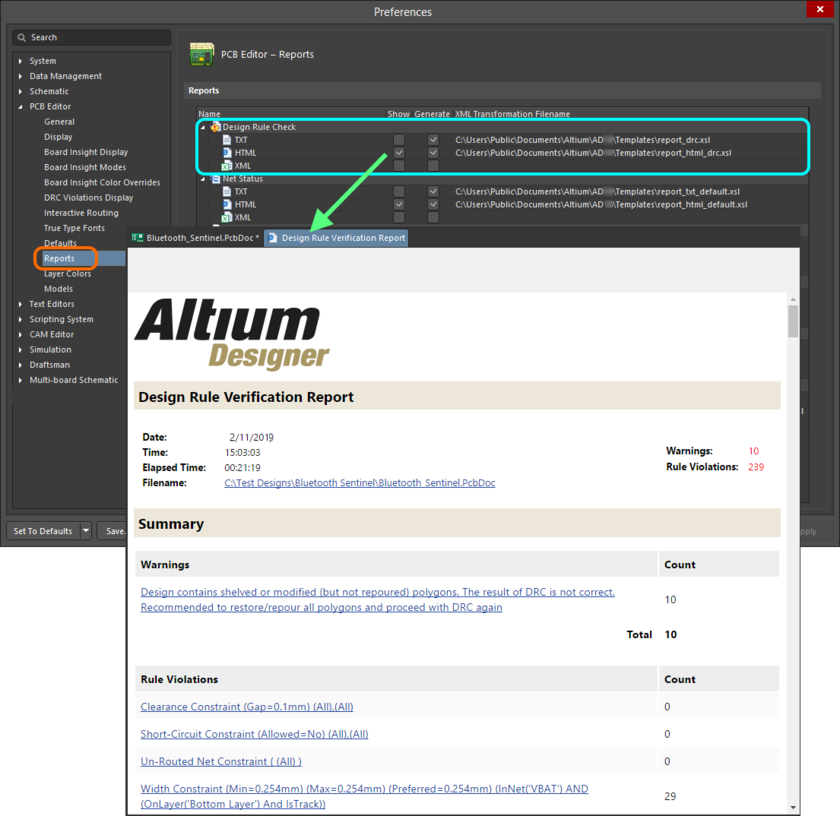
Design Rule Checking Altium Designer 19 0 User Manual Documentation
Source : pinterest.com
